ADRF5549 Receiver Front End, Dual-Channel, 1.8 GHz to 2.8 GHz
Product Details
The ADRF5549 is a dual-channel, integrated, RF front-end multichip module designed for time division duplexing (TDD) applications that operates from 1.8 GHz to 2.8 GHz. The ADRF5549 is configured in dual channels with a cascading, two-stage, low noise amplifier (LNA) and a high power, silicon single-pole, double-throw (SPDT) switch.
In high gain mode, the cascaded two-stage LNA and switch offer a low noise figure of 1.4 dB and a high gain of 35 dB with an output third-order intercept point (OIP3) of 32 dBm typical.
In low gain mode, one stage of the two-stage LNA is in bypass mode providing 17 dB of gain at a lower current of 35 mA. In power-down mode, the LNAs are turned off, and the device draws 12 mA.
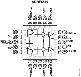
In transmit operation, when RF inputs are connected to a termination pin (TERM-ChA or TERM-ChB), the switch provides a low insertion loss of 0.6 dB and handles a long-term evolution (LTE) full lifetime average (9 dB peak to average ratio (PAR)) of 40 dBm and 43 dBm for a 9 dB PAR LTE single event (<10 sec) average. The device comes in a RoHS-compliant, compact, 6 mm × 6 mm, 40-lead, lead frame chip-scale package (LFCSP).
Applications
- Wireless Infrastructure
- TDD massive multiple input and multiple output (MIMO) and active antenna systems
- TDD-based communication systems
Features and Benefits
- Integrated dual-channel RF front end
- 2-stage LNA and high power SPDT switch
- On-chip bias and matching
- Single-supply operation
- Gain
- High gain mode: 35 dB typical at 2.3 GHz
- Low gain mode: 17 dB typical at 2.3 GHz
- Low noise figure
- High gain mode: 1.4 dB typical at 2.3 GHz
- Low gain mode: 1.4 dB typical at 2.3 GHz
- High isolation
- Between RxOUT-ChA and RxOUT-ChB: 50 dB typical
- Between TERM-ChA and TERM-ChB: 62 dB typical
- Low insertion loss: 0.6 dB typical at 2.3 GHz
- High power handling at TCASE = 105°C
- Full lifetime
- LTE average power (9 dB PAR): 40 dBm
- Single event (<10 sec operation)
- LTE average power (9 dB PAR): 43 dBm
- Full lifetime
- High OIP3: 32 dBm typical
- Power-down mode and low gain mode for LNA
- Low supply current
- High gain mode: 85 mA typical at 5V
- Low gain mode: 35 mA typical at 5 V
- Power-down mode: 12 mA typical at 5 V
- Positive logic control
- 6 mm × 6 mm, 40-lead LFCSP